数字IC笔试题 ——全志科技数字前端
转:https://blog.csdn.net/bleauchat/article/details/91383913
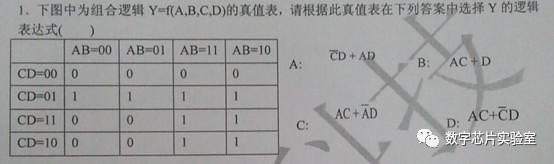
D
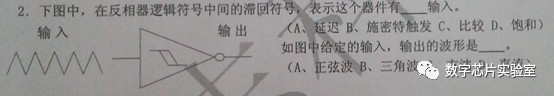
B、施密特触发
C、方波
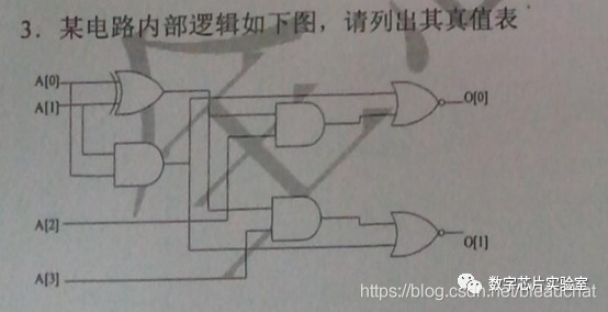
列出所有情况A[3:0] = 4’b0000 ~ 4’b1111即可
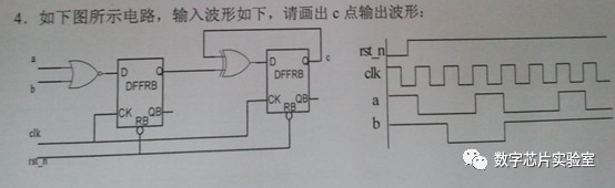
rst_n为异步复位,然后在每个clk上升沿进行触发器状态更新
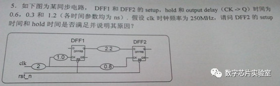
时钟路径:0.8ns
数据路径:1+1.2+2.2=4.4ns 时钟周期T=4ns
建立检查:数据要求最晚到达时间为 0.8+4-Tsu=4.2ns<4.4 所以建立时间违例
保持检查:数据要求最早到达时间为 0.8+Th=1.1ns <4.4 所以保持时间满足

所谓分频器就是计数器的输出状态,奇数分频器需要同时用到上升沿和下降沿。
根据输入寄存器控制分频计数值
module divider( input clk , input rst_n , input [2:0] divider_num , output reg out_clk); reg [2:0] divider_num_reg ; always@(posedge clk or negedge rst_n) beginif(!rst_n) begin divider_num_reg <= 0 ;endelse begin divider_num_reg <= divider_num ;end end reg [2:0] count ; always@(posedge clk or negedge rst_n) beginif(!rst_n) begin count <= 0 ; out_clk <= 0 ; endelse begin count <= count +1 ; if(count == (divider_num_reg-1))begin out_clk <= ~out_clk ; count <= 0 ; end end end always@(negedge clk or negedge rst_n) beginif(!rst_n) begin count <= 0 ; out_clk <= 0 ;endelse begin count <= count +1 ; if(count == (divider_num_reg-1))begin out_clk <= ~out_clk ; count <= 0 ; end end end endmodule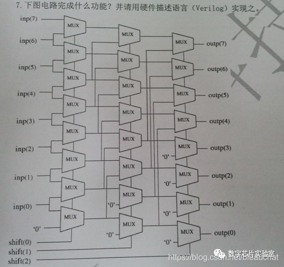
module shift_mux( input [7:0] inp , input [2:0] shift, output reg [7:0] outp); always@(*) begin case(shift) 3'b000: assign outp ={inp[0],7'b000_0000} ; 3'b001: assign outp ={inp[1],inp[0],6'b00_0000} ; 3'b010: assign outp ={inp[2],inp[1],inp[0],5'b0_0000} ; 3'b011: assign outp ={inp[3],inp[2],inp[1],inp[0],4'b0000} ; 3'b100: assign outp ={inp[4],inp[3],inp[2],inp[1],inp[0],3'b000} ; 3'b101: assign outp ={inp[5],inp[4],inp[3],inp[2],inp[1],inp[0],2'b00} ; 3'b110: assign outp ={inp[6],inp[5],inp[4],inp[3],inp[2],inp[1],inp[0],1'b0} ; 3'b111: assign outp ={inp[7],inp[6],inp[5],inp[4],inp[3],inp[2],inp[1],inp[0]} ; endcase endendmodule
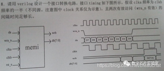
module interface_change( input clka , input wra_n, input da , inputclkb , output [7:0] db , outputwrb); reg [7:0] data = 0 ;always@(posedge clka) begin if(!wra_n)begin data<= {data[6:0],da} ; endend reg wra_n_reg1 ,wra_n_reg2 ;always@(posedge clkb ) begin wra_n_reg1<= wra_n ; wra_n_reg2<= wra_n_reg1 ;end wire wra_n_check ;assign wra_n_check = wra_n_reg1&&(!wra_n_reg2) ;assign wrb = wra_n_check ;assign db = (wra_n_check == 1'b1) ? data :0 ;