FPGA学习笔记3.1——七段管实现字符序列移位
设计思路
SW上拨为输出高电平、下拨为输出低电平,由其控制左移还是右移
在8个7段管上显示HELLO_ _ _(可以显示下划线或不亮也可),每隔1秒钟,字符序列左移或右移一个七段管的位置。系统外部时钟50Mhz
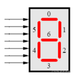
原理图

功能模块代码:
module Hello(clk50,sw,clk1,out0,out1,out2,out3,out4,out5,out6,out7); input clk50,sw; output wire clk1; output reg[6:0] out0=7'b1110110; //显示H output reg[6:0] out1=7'b1111001; //显示E output reg[6:0] out2=7'b0111000; //显示L output reg[6:0] out3=7'b0111000; //显示L output reg[6:0] out4=7'b0111111; //显示O output reg[6:0] out5=7'b0000000; //不显示 output reg[6:0] out6=7'b0000000; //不显示 output reg[6:0] out7=7'b0000000; //不显示 clk50to1 test(clk50,clk1); always@(posedge clk1) begin if(sw) begin out0<=out1; out1<=out2; out2<=out3; out3<=out4; out4<=out5; out5<=out6; out6<=out7; out7<=out0; end else begin out7<=out6; out6<=out5; out5<=out4; out4<=out3; out3<=out2; out2<=out1; out1<=out0; out0<=out7; end endendmodulemodule clk50to1(clk50,clk1); input wire clk50; output reg clk1=1; integer i=0; always@(posedge clk50) begin if(i==25000000) begin i=0; clk1=~clk1; end else begin i=i+1; end endendmodule 测试模块代码:
// Copyright (C) 2017 Intel Corporation. All rights reserved.// Your use of Intel Corporation's design tools, logic functions // and other software and tools, and its AMPP partner logic // functions, and any output files from any of the foregoing // (including device programming or simulation files), and any // associated documentation or information are expressly subject // to the terms and conditions of the Intel Program License // Subscription Agreement, the Intel Quartus Prime License Agreement,// the Intel FPGA IP License Agreement, or other applicable license// agreement, including, without limitation, that your use is for// the sole purpose of programming logic devices manufactured by// Intel and sold by Intel or its authorized distributors. Please// refer to the applicable agreement for further details.// *// This file contains a Verilog test bench template that is freely editable to // suit user's needs .Comments are provided in each section to help the user // fill out necessary details. // *// Generated on "04/07/2022 09:57:01" // Verilog Test Bench template for design : Hello// // Simulation tool : ModelSim-Altera (Verilog)// `timescale 1 ps/ 1 psmodule Hello_vlg_tst();// constants // general purpose registersreg eachvec;// test vector input registersreg clk50;reg sw;integer i=0;// wires wire clk1;wire [6:0] out0;wire [6:0] out1;wire [6:0] out2;wire [6:0] out3;wire [6:0] out4;wire [6:0] out5;wire [6:0] out6;wire [6:0] out7;parameter DELY=20;always #(DELY/2) clk50=~clk50;// assign statements (if any) Hello i1 (// port map - connection between master ports and signals/registers .clk1(clk1),.clk50(clk50),.out0(out0),.out1(out1),.out2(out2),.out3(out3),.out4(out4),.out5(out5),.out6(out6),.out7(out7),.sw(sw));initial begin // code that executes only once // insert code here --> begin // --> end $display("Running testbench"); clk50=0; sw=1;end always// optional sensitivity list // @(event1 or event2 or .... eventn) begin // code executes for every event on sensitivity list // insert code here --> begin @eachvec; // --> end end endmodule运行图:
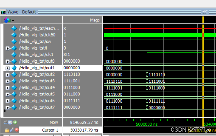
(mnitor数据图随后更新)
注意clk50的变化