FPGA学习笔记3.2——用Verilog实现七段管计时器
设计思路
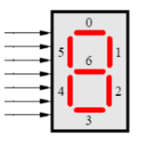
在6个七段管上分别显示 小时(0-23或11)、分(0-59)、秒(0-59),各占2个管。外部时钟50Mhz。可以用按键来产生一个复位信号key,当按键按下立刻(异步)将时间复位成0小时、0分、0秒重新开始计时
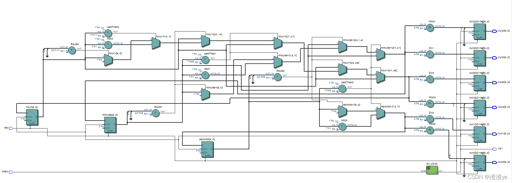
原理图
功能模块代码:
module Cllo(clk50,key,clk1,out5,out4,out3,out2,out1,out0); input clk50,key;// clk50:输入50MHz信号;key:异步复位信号 output clk1;// clk1:新产生的1Hz信号 output reg [6:0] out5;// 输出,时_十位 output reg [6:0] out4;// 输出,时_个位 output reg [6:0] out3; // 输出,分_十位 output reg [6:0] out2;// 输出,分_个位 output reg [6:0] out1;// 输出,秒_十位 output reg [6:0] out0;// 输出,秒_个位 reg [6:0] hour=0;// 计数器_时(0-23) reg [6:0] minutes=0;// 计数器_分(0-59) reg [6:0] seconds=0;// 计数器_秒(0-59) div_clk dc(clk50,clk1);// 模块调用,50MHz -> 1Hz// clk1,上升沿触发;key,异步信号,高电平有效 always@(posedge clk1,posedge key) begin // 异步复位 if(key) begin hour=0;minutes=0;seconds=0; // 直接输出,方便观察检验结果 // 若连接7段管,输出信号用任务 dec_out 转换即可 // dec_out(输入:十进制数 , 输出:7位二进制数值,对应7段管显示) // 例:dec_out(hour/10,out5); out5=hour/10; out4=hour%10; out3=minutes/10; out2=minutes%10; out1=seconds/10; out0=seconds%10; end // 计数 else begin if(seconds<59) seconds=seconds+1; else beginif(seconds==59) begin seconds=0; if(minutes<59) minutes=minutes+1; else begin if(minutes==59) begin minutes=0; if(hour 1Hz// 50MHz = 2*10^-8 s = 20ns// 1Hz = 1s// 1s/20ns = 5*10^7,即1Hz信号的一个周期包含50MHz信号的5*10^7个周期// (5*10^7)/2 = 25000000,产生1Hz信号时,每过25000000个周期翻转一次module div_clk(clk50,clk1); input clk50;// clk50:输入的50MHz信号 output reg clk1=1;// clk1: 产生的1Hz信号,赋初始值为1 integer i=0;// 50MHz频率下,周期计数器 always@(posedge clk50) // clk50上升沿触发 begin if(i==250)// 每过25000000个周期 begini=0;clk1=~clk1;// clk1翻转 end else i=i+1; end endmodule 测试模块代码:
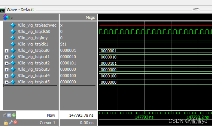
// Copyright (C) 2017 Intel Corporation. All rights reserved.// Your use of Intel Corporation's design tools, logic functions // and other software and tools, and its AMPP partner logic // functions, and any output files from any of the foregoing // (including device programming or simulation files), and any // associated documentation or information are expressly subject // to the terms and conditions of the Intel Program License // Subscription Agreement, the Intel Quartus Prime License Agreement,// the Intel FPGA IP License Agreement, or other applicable license// agreement, including, without limitation, that your use is for// the sole purpose of programming logic devices manufactured by// Intel and sold by Intel or its authorized distributors. Please// refer to the applicable agreement for further details.// *// This file contains a Verilog test bench template that is freely editable to // suit user's needs .Comments are provided in each section to help the user // fill out necessary details. // *// Generated on "04/07/2022 10:37:27" // Verilog Test Bench template for design : Cllo// // Simulation tool : ModelSim-Altera (Verilog)// `timescale 1 ps/ 1 psmodule Cllo_vlg_tst();// constants // general purpose registersreg eachvec;// test vector input registersreg clk50;reg key;// wires wire clk1;wire [6:0] out0;wire [6:0] out1;wire [6:0] out2;wire [6:0] out3;wire [6:0] out4;wire [6:0] out5;// assign statements (if any) Cllo i1 (// port map - connection between master ports and signals/registers .clk1(clk1),.clk50(clk50),.key(key),.out0(out0),.out1(out1),.out2(out2),.out3(out3),.out4(out4),.out5(out5));// 产生时钟信号 // 一个时钟周期为20ns parameter DELAY=20; // 半个周期翻转一次 always #(DELAY/2) clk50=~clk50;initial begin // code that executes only once // insert code here --> begin // --> endclk50=0;key=0; $display("Running testbench"); end always// optional sensitivity list // @(event1 or event2 or .... eventn) begin // code executes for every event on sensitivity list // insert code here --> begin $monitor($realtime,,,"%d %d : %d %d : %d %d",out5,out4,out3,out2,out1,out0); @eachvec; // --> end end endmodule运行图:

下午继续改进