GD32硬件IIC
GD32E230硬件IIC
我们熟悉IIC都是使用软件代码的形式模拟时序图来编程
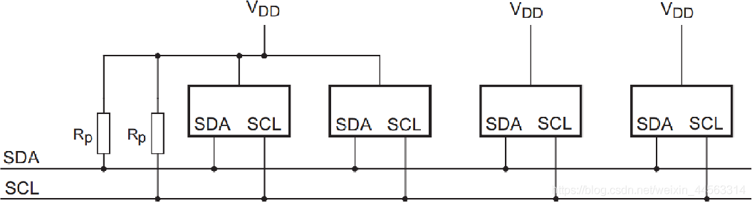
现在使用GD32E230中的HAL库中硬件IIC模式IIC。的总线机制都是一种两线接口、简单、双向二线制同步的串行总线,二线制就是时钟线(SCL)和数据线(SDA)两个信号线。IIC寻址时分为主从设备之分,一般选择MCU作为主设备,每个不同的从设备都有唯一的7位设备地址,高四位由厂家确定,低三位时器件引脚定义。
IIC通信时,存在几种信号。
1)起始信号:通知从机做好通信准备。
2)应答信号:有应答和无应答信号。有答应就是SDA为低电平,无应答就是SDA为高电平。
3)停止信号:告诉从机通信结束
首先编写硬件IIC时,要根据厂家提供的规格书来编写,一般都遵循IIC标准通信时序进行通信。
传输方向都是一致的
1)首先 是选择主从设备,大部分情况下都会选择单片机(MCU)作为主设备
2)主设备要发送数据给从器件,主设备首先寻址从设备,主动发送数据给从设备,最后由主机终止数据传送。
3)如果主机要接收从器件的数据,首先由主器件寻址从器件.然后主机接收从器件发送的数据,最后由主机终止接收过程。在这种情况下,主机负责产生定时时钟和终止数据传送。
IIC的写数据
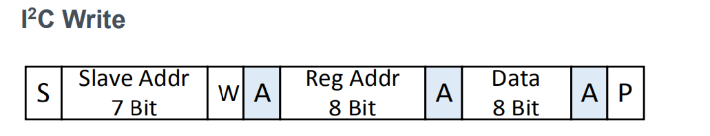
看到规格书里面的表达时,先从左边开始编写
S(起始信号)通信的开始
while(i2c_flag_get(I2C0, I2C_FLAG_I2CBSY)); /* send a start condition to I2C bus */ i2c_start_on_bus(I2C0); /* wait until SBSEND bit is set */ while(!i2c_flag_get(I2C0, I2C_FLAG_SBSEND));Slave Addr 7 Bit(设备寻址)
/* send slave address to I2C bus */ i2c_master_addressing(I2C0, 0x70, I2C_TRANSMITTER);//我这边的设备地址是0c70 /* wait until ADDSEND bit is set */ while(!i2c_flag_get(I2C0, I2C_FLAG_ADDSEND)); /* clear the ADDSEND bit */ i2c_flag_clear(I2C0,I2C_FLAG_ADDSEND);W(等待应答信号)
A(应答信号)
/* wait until the transmit data buffer is empty */ while( SET != i2c_flag_get(I2C0, I2C_FLAG_TBE));Reg Addr 8 Bit(寄存器的8位地址)这个地址是读写数据时都要一致
/* send the reg internal address to write to */ i2c_data_transmit(I2C0, 0x1c);//这个地址是读写数据时都要一致 /* wait until BTC bit is set */ while(!i2c_flag_get(I2C0, I2C_FLAG_BTC));Data 8 Bit(II2SDA数据线上的8位数据)
writ_byte = writ_byte << 1; i2c_data_transmit(I2C0, writ_byte); /* wait until BTC bit is set */ while(!i2c_flag_get(I2C0, I2C_FLAG_BTC));P(停止信号)
/* send a stop condition to I2C bus */ i2c_stop_on_bus(I2C0); /* wait until the stop condition is finished */ while(I2C_CTL0(I2C0)&0x0200);II2的读数据
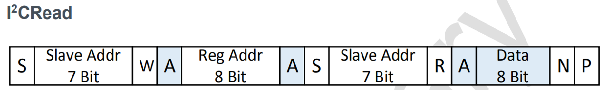
S(起始信号)通信的开始
while(i2c_flag_get(I2C0, I2C_FLAG_I2CBSY)); /* send a start condition to I2C bus */ i2c_start_on_bus(I2C0); /* wait until SBSEND bit is set */ while(!i2c_flag_get(I2C0, I2C_FLAG_SBSEND));Slave Addr 7 Bit(设备寻址)
/* send slave address to I2C bus */ i2c_master_addressing(I2C0, 0x70, I2C_TRANSMITTER);//我这边的设备地址是0c70 /* wait until ADDSEND bit is set */ while(!i2c_flag_get(I2C0, I2C_FLAG_ADDSEND)); /* clear the ADDSEND bit */ i2c_flag_clear(I2C0,I2C_FLAG_ADDSEND);W(等待应答信号)
A(应答信号)
/* wait until the transmit data buffer is empty */ while( SET != i2c_flag_get(I2C0, I2C_FLAG_TBE)); /* enable I2C0*/ i2c_enable(I2C0);Reg Addr 8 Bit(寄存器的8位地址)这个地址是读写数据时都要一致
/* send the reg internal address to write to */ i2c_data_transmit(I2C0, 0x1c);//这个地址是读写数据时都要一致 /* wait until BTC bit is set */ while(!i2c_flag_get(I2C0, I2C_FLAG_BTC));S(起始信号)
/* wait until BTC bit is set */ while(!i2c_flag_get(I2C0, I2C_FLAG_BTC)); /* send a start condition to I2C bus */ i2c_start_on_bus(I2C0); /* wait until SBSEND bit is set */ while(!i2c_flag_get(I2C0, I2C_FLAG_SBSEND));Slave Addr 7 Bit(设备寻址)
/* send slave address to I2C bus */ i2c_master_addressing(I2C0, 0x70, I2C_RECEIVER);//我这边的设备地址是0c70 /* wait until ADDSEND bit is set */ while(!i2c_flag_get(I2C0, I2C_FLAG_ADDSEND)); /* clear the ADDSEND bit */ i2c_flag_clear(I2C0,I2C_FLAG_ADDSEND);Data 8 Bit(II2SDA数据线上的8位数据)
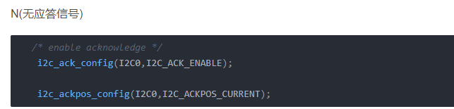
*p_buffer = i2c_data_receive(I2C0); /* point to the next location where the byte read will be saved */ p_buffer++; N(无应答信号)
/* enable acknowledge */ i2c_ack_config(I2C0,I2C_ACK_ENABLE); i2c_ackpos_config(I2C0,I2C_ACKPOS_CURRENT);P(停止信号)
/* send a stop condition to I2C bus */ i2c_stop_on_bus(I2C0); /* wait until the stop condition is finished */ while(I2C_CTL0(I2C0)&0x0200);最后需要注意的是
1、读写的时候一定的寄存器一定要填写一致并且,还有规格书上的设备地址需要左移一位,因为IIC的设备地址是高八位开始。
2、read byte时,当发送完slave addr时要再次启动i2c总线时,一定要给出无应答信号,不然数据数据读取不到。
最后还有问题不懂或者文章有错的评论区告诉我。谢谢!需要GD32E230标准HAL库私聊。
…