FPGA: UltraScale+ bitslip实现(方案+代码)_bitslip原理
收获
一晃五年~
五年前那个夏夜,我对着泛蓝的屏幕敲下《给十年后的自己》,在2020年的疫情迷雾中编织着对未来的想象。此刻回望,第四届集创赛的参赛编号仍清晰如昨,而那个在家熬夜焊电路板的\"不眠者\",现在也渐渐熬不动夜了😹😹
如果遇见五年前的自己,我想告诉他:当年在博客里追问的\"职业门路\",答案就藏在每个调试通宵的星光里;那些担心被时代抛下的焦虑,终会熔铸成攀登技术栈的勇气。🙆🙆
十年之约才过半程,职业的时钟域仍在扩展,就像我们永远年轻的技术信仰。下一个五年,愿芯片上的每一个逻辑门都通往星辰,愿每个深夜的坚持都能被未来温柔解码——因为代码从不辜负时光,正如奋斗永远眷顾追梦人。🍃 🍃

目录
- 收获
- 正文
-
- 1、参考文献
- 2、Bitslip in Logic
-
- 2.1、现状
- 2.2、bitslip原理
- 2.3、解决方案A
- 2.4、解决方案B
-
- 2.4.1、8B verilog代码:
- 2.4.2、分析一下代码
- 3、RX_BITSLICE功能
- 4、工程获取
-
- 4.1、部分代码
- 4.2、完整工程(含仿真)
- 总结
正文
1、参考文献
本文主要讲UltraScale+ bitslip方案,iserdese3等概念,有文章说过了,这里就不做赘述:
1、Ultrascale selectio 仿真之 ISERDESE3和OSERDESE3
2、ISERDESE3/OSERDESE3例化和仿真
3、LVDS系列11:Xilinx Ultrascale系可编程输入延迟(一)
4、Xilinx IDELAYE3原语详细解读
5、iodelay 使用总结
(5这篇参数比较详细)
本文工程会放在最后一节。
注意:
一些争议点:
ISERDESE3有个地方,xilinx手册可能有点歧义:
从手册看,Q[7:0]的输出是占了2个CLKDIV时钟周期,但是实际仿真,只占了1个。
不管是其他博主的仿真,还是我自己仿的,都是1个clkdiv周期,有知道的朋友,可以评论区留言交流。
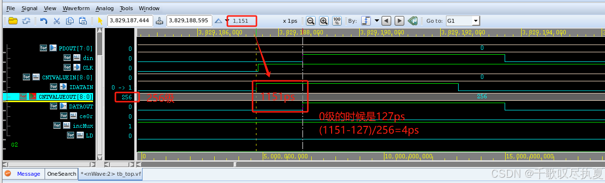
看了几篇文章,每篇文章一个tap多少ps说的总是有些出入,这里结合我的仿真,算了一下,一个tap是4ps(事实上,我在一个器件文档里面是有提到硬件决定了这就是4ps的,但是忘记哪个文档了):
0级的时候,输入和输出直接的延迟是127ps;后面每次算,都要减去或者加上这个127ps。
有其他看法的朋友,也可以评论区交流。
2、Bitslip in Logic
2.1、现状
这小节结论:ISERDESE3没有bitslip功能了,需要用逻辑实现。(可以结合小结3的RX_BITSLICE结构图看一下)
UltraScale器件中的I/O逻辑是指位于专用的I/O处理组件在I/O缓冲区和一般互连之间。这个I/O逻辑在UltraScale中是不同的。与以前的系列(如7系列和Virtex-6 fpga)相比,UltraScale器件中的I/O逻辑设置提供更快的I/O处理,更好的抖动规格,还有更多的功能。但是,它忽略了以前器件系列的I/O逻辑中可用的一些功能。
位滑(bitslip)是一个在UltraScale器件I/O逻辑中原生不可用的功能。这个应用程序注描述了在一般互连中实现的位滑解决方案,可用于超规模的设备组件以及以前的设备架构。
参考设计实现了位滑函数,并扩展了几个额外的基本功能选项。使用基本的 UltraScale 器件 BITSLICE I/O 原语被称为“本机模式(native mode)”,而使用具有“组件模式(component mode)”原语的 UltraScale 器件 I/O 来模仿以前设备系列的 I/O 逻辑功能。
位滑函数在以前的器件系列的每个ISERDES中都是本地可用的,它作用于串行输入流。
在UltraScale器件中,ISERDES等效(组件模式)或 本机RX_BITSLICE函数没有实现Bitslip功能。
本应用说明描述了以前的设备系列中原生支持的Bitslip功能,以及如何在UltraScale设备中实现等效的Bitslip。
参考设计将所描述的解决方案作为现成的设计提供,可以在必要时进行修改。所提供的参考设计可用于具有4位和8位输出的组件模式(ISERDES)或本机模式(RX_BITSLICE),并且可以使用VHDL代码中的“属性/泛型”进行自定义。参考设计也可以用于7系列和Virtex-6 FPGA设计,这可以使设计的重新定位更容易。修改原始设计,使用通用互连实现的Bitslip代替原生Bitslip。在原始设备技术中测试设计后,将其移植到UltraScale设备中。
在逻辑中实现的Bitslip功能的组件块下图所示。此块及其引脚和属性将在本文档后面详细解释。

注意:
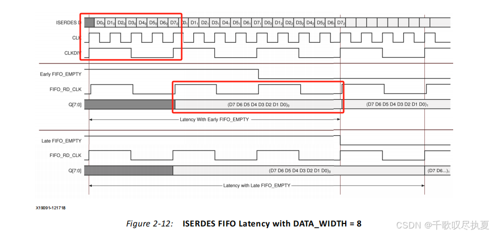
讲bitslip之前,我觉得有必要插入CLKDIV概念:
CLKDIV 是 CLK 的分频版本。当 DATA_WIDTH 设置为 8 且 ISERDES 用于单数据速率 (SDR) 模式时,CLKDIV 为 CLK 的 8 分频。当 ISERDES 用于双数据速率 (DDR) 模式时,CLKDIV 为 CLK 的 4 分频。
假设DATA_WIDTH 设置为 8:
- 以 CLK 速率将位捕获到 ISERDES 的输入串并寄存器中。
- ISERDES 中以相同 CLK 运行的状态机每次达到 DATA_WIDTH 设置的值时,都会生成一个时钟脉冲,将串并寄存器中的位捕获到内部寄存器中。在这种情况下,当串并寄存器中捕获到 8 位时,状态机就会为内部寄存器生成一个时钟脉冲。
- 内部状态机生成的时钟等效于外部提供的 CLKDIV 时钟。该内部生成的时钟与 CLK 时钟相关,且与外部施加的 CLKDIV 时钟相位不一致。
- 数据通过外部应用的 CLKDIV 时钟从内部寄存器传输到并行输出寄存器 Q。
2.2、bitslip原理
(本节如果看起来抽象,可以看看这篇文章:xilinx原语详解及仿真之ISERDESE)
图 2(SDR 操作)显示了一个功能示例。数据采集从位值 7 开始。位以 CLK 时钟速率移入串并寄存器。垂直堆叠的块代表该寄存器。这些块显示值为 7 的位首先移入,然后移至底部。最后移入的位是值为 D 的位。当串并寄存器包含八个采集位时,内部寄存器会采集其中的内容。在下一个 CLKDIV 上升沿,内容移至并行输出寄存器。该寄存器随后包含值 DCBA0987。
(不是你屏幕长蚊子了,是我翻译贴图了😹)
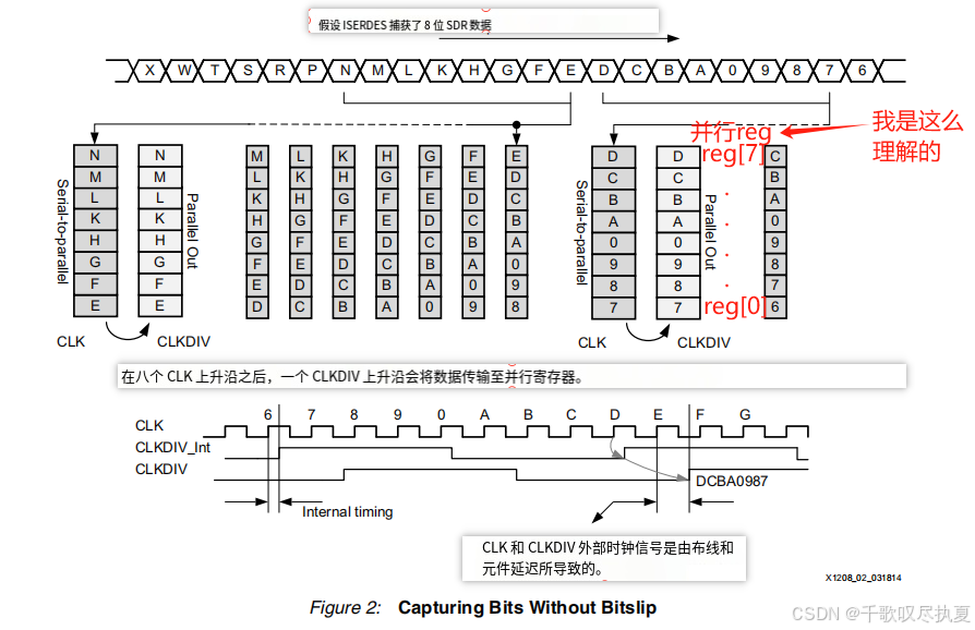
一旦数据从串行到并行寄存器被转移到内部存储寄存器,连续的新数据就被转移到串行到并行寄存器中。
当使用Bitslip功能时,捕获、传输到内部寄存器和传输到输出寄存器的操作方式相同。
当ISERDES位滑输入信号被断言时,在串行到并行寄存器和内部寄存器之间的数据传输延迟一个CLK周期。
当数据传输延迟一个CLK周期时,一个额外的位被移到串行-并行寄存器中,另一端丢失一个位。
当数据在内部寄存器中被捕获时,看起来好像数据被移动了一位。图3显示了与图2相同的行为,除了在串行到并行寄存器中捕获第二个字节时执行Bitslip操作。数据不是在捕获第8位之后传输到并行寄存器,而是在捕获第9位之后。看起来好像图案移动了一位。在串行-并行寄存器的底部(末尾),移位的第一个位丢失。
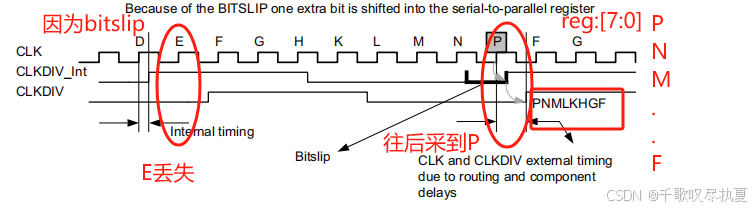
每次BITSLIP输入保持高位超过半个CLKDIV周期,就对数据执行一次BITSLIP操作。连续捕获相同的输入位模式会导致位的移位。因此,这种机制可以很容易地用于将数据与模式对齐,或将一个数据通道与另一个数据通道对齐。
Bitslip 功能也可以在 I/O 逻辑的输出端使用通用互连来实现。这意味着该功能必须对并行反序列化数据执行,而不是像在先前架构中(7系列FPGA)的原生 Bitslip 功能中解释的那样,对输入的串行数据执行。
本文提供了一种电路,可以以 CLKDIV 速率对并行数据字中的位进行 Bitslip 或移位。可以构建几种可能的电路来执行此操作。
2.3、解决方案A
现在介绍一种动态移位和预定移位解决方案。
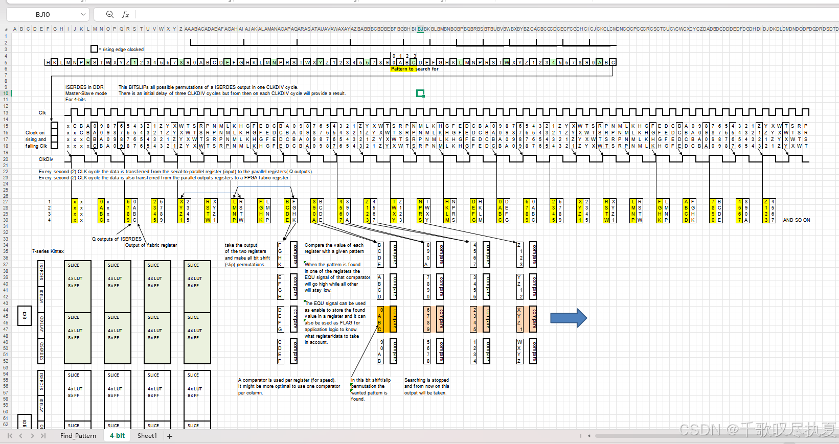
以CLKDIV速率旋转串行顺序并行寄存器中的位。为了在所有可能性中进行位滑或移位,它将占用与寄存器宽度一样多的CLKDIV时钟周期
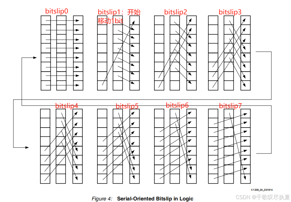
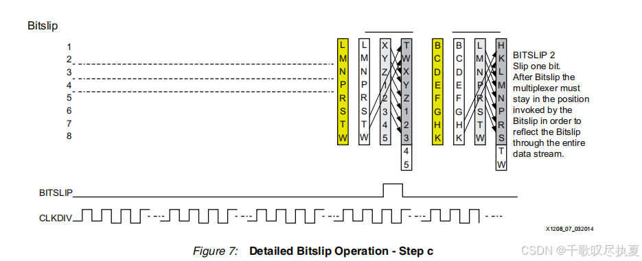
图4显示了8位字上所有可能的移位或位滑步。要执行这些操作,至少需要两个8位寄存器和一个多路复用器。图5到图7详细显示了当执行单个Bitslip步骤时发生的情况。
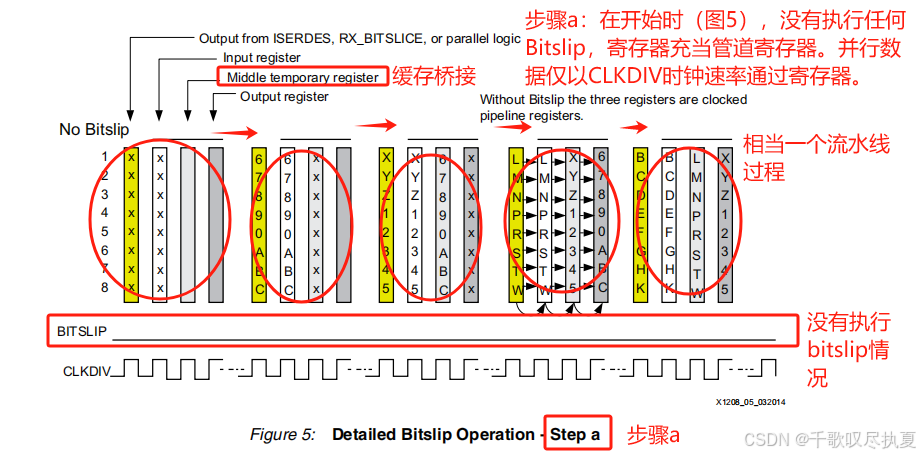
觉得下面这个图抽象不好理解的,可以结合2.2节第二个图理解。
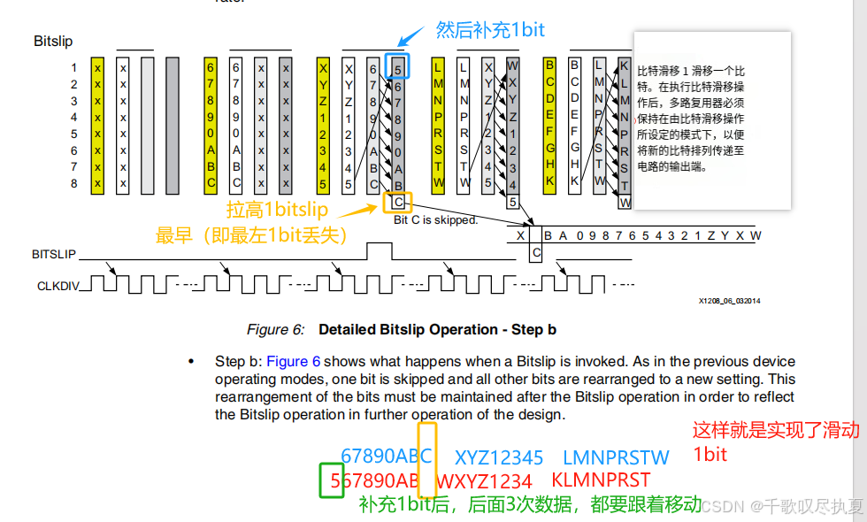
Step C,原理跟上面Step B一样,只不过每次可以滑动2bit。
布局布线后框图:
2.4、解决方案B
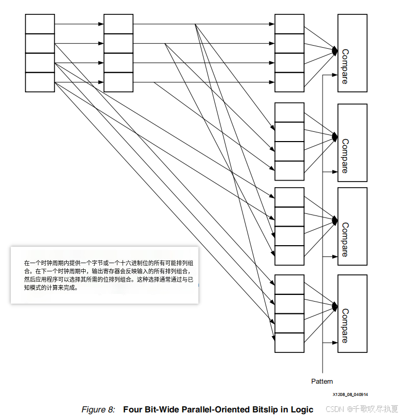
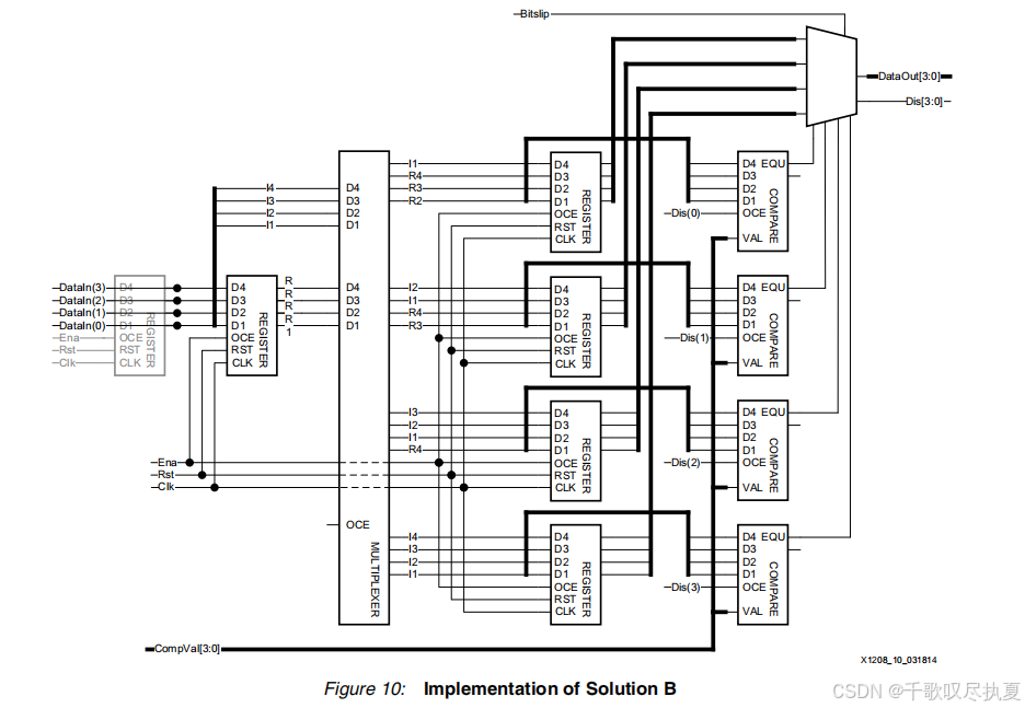
获取ISERDES、RX_BITSLICE或其他并行逻辑的输出,并将所有位同时旋转到一组并行放置的寄存器中。该解决方案需要一个CLKDIV循环来遍历所有可能的值。在操作开始时,需要两个时钟周期来获得有效的输出:一个初始时钟周期用于加载历史寄存器,第二个时钟周期用于加载输出寄存器中的所有位排列。从那时起,每个时钟周期都会产生有效的输出数据。然后,应用程序可以选择具有所需位排列的小块或字节。当必须检测和匹配预先确定的模式时,此解决方案是理想的(参见图8)。
框图与代码(2.4.1小节)的对应关系
从框图中可以看到:
左侧的4个方块对应代码中的输入寄存器(IntRankOne)
中间的4个方块对应位移寄存器(IntRankTwo)和位移逻辑
右侧的多组寄存器和比较器对应于多种位移配置
\"Compare\"模块对应于代码中的比较逻辑
这个表格,就是上面框架图4bit的。
整个代码框架:
┌─────────────┐ ┌─────────────┐ ┌─────────────┐ ┌─────────────┐│ 输入数据 │ │ 位移逻辑 │ │ 比较与选择 │ │ 输出 ││ DataIn_pin │───►│生成所有排列 │───►│ 根据模式选择│───► │ DataOut_pin │└─────────────┘ └─────────────┘ └─────────────┘ └─────────────┘ │ ▲ ▲ │ │ │ │ ┌─────────────┐ ┌─────────────┐ └───────────►│ 控制逻辑 │ │ 比较模式 │ │ (模式选择) │◄───│ CompVal_pin │ └─────────────┘ └─────────────┘双缓冲寄存器结构框架:
┌───────────┐ ┌───────────┐ ┌───────────┐│ IntRankOne│ │ IntRankTwo│ │ IntRankTre││ 当前输入 │──────►│ 前一周期 │──────►│ 输出寄存 │└───────────┘ └───────────┘ └───────────┘ │ │ ▲ │ │ │ └────────┬───────────┘ │ ▼ │ ┌───────────────────────┐ │ │ 位移多路复用器 │ │ │ (组合逻辑电路) │────────────────┘ └───────────────────────┘2.4.1、8B verilog代码:
`timescale 1ns / 1psmodule BitSlipInLogic_8b #( parameter C_Function = \"Slip\", // Slip, Nmbr, Comp parameter C_ErrOut = 1, // 1 = ErrOut pin available. parameter C_InputReg = 0 // 0, No, 1 = Yes) ( input wire [7:0] DataIn_pin, input wire Bitslip_pin, input wire [2:0] SlipVal_pin, input wire [7:0] CompVal_pin, input wire Ena_pin, input wire Rst_pin, input wire Clk_pin, output wire [7:0] DataOut_pin, output wire ErrOut_pin);// Constantslocalparam Low = 1\'b0;localparam High = 1\'b1;// Signalsreg [7:0] IntBitSlipPosition;reg IntFrstBitSlipPstn;reg [7:0] IntBitSlipData;wire [7:0] IntRankOne;reg [7:0] IntRankTwo;reg [7:0] IntRankTre;wire IntEnaReg;reg IntEnaReg_d;wire IntShftSlipReg;reg IntSlipPulse_d;reg IntShiftEna_d;wire IntSlipPulse;wire IntShiftEna;wire IntShftCntTc;wire IntShftCntEna;wire IntCompEqu;reg IntCompEqu_d;wire IntCompEqu_Rst;wire IntShftCntRst;wire [2:0] IntBitSlipCntOut;wire IntErrOut;reg IntErrOut_d;// Attributes(* KEEP_HIERARCHY = \"YES\" *) wire _unused_;////////////////////////////////////////////////////////////////////////////////////////////// Extra front input register.// Adds one pipeline stage!////////////////////////////////////////////////////////////////////////////////////////////generate if (C_InputReg == 1) begin : Gen_1_0 reg [7:0] IntRankOne_reg; always @(posedge Clk_pin or posedge Rst_pin) begin if (Rst_pin) IntRankOne_reg <= 8\'b00000000; else if (Ena_pin) IntRankOne_reg <= DataIn_pin; end assign IntRankOne = IntRankOne_reg; end else begin : Gen_1_1 assign IntRankOne = DataIn_pin; endendgenerate////////////////////////////////////////////////////////////////////////////////////////////// These are the bitslip registers.////////////////////////////////////////////////////////////////////////////////////////////always @(posedge Clk_pin or posedge Rst_pin) begin if (Rst_pin) begin IntRankTwo <= 8\'b00000000; IntRankTre <= 8\'b00000000; end else begin if (Ena_pin) IntRankTwo <= IntRankOne; if (IntEnaReg) IntRankTre <= IntBitSlipData; endendassign DataOut_pin = IntRankTre;// Mux logic for bit slippingalways @(*) begin case({Ena_pin, IntBitSlipPosition}) 9\'b100000000: IntBitSlipData = IntRankOne[7:0]; 9\'b100000001: IntBitSlipData = {IntRankOne[0], IntRankTwo[7:1]}; 9\'b100000010: IntBitSlipData = {IntRankOne[1:0], IntRankTwo[7:2]}; 9\'b100000100: IntBitSlipData = {IntRankOne[2:0], IntRankTwo[7:3]}; 9\'b100001000: IntBitSlipData = {IntRankOne[3:0], IntRankTwo[7:4]}; 9\'b100010000: IntBitSlipData = {IntRankOne[4:0], IntRankTwo[7:5]}; 9\'b100100000: IntBitSlipData = {IntRankOne[5:0], IntRankTwo[7:6]}; 9\'b101000000: IntBitSlipData = {IntRankOne[6:0], IntRankTwo[7]}; 9\'b110000000: IntBitSlipData = IntRankOne[7:0]; default: IntBitSlipData = 8\'b00000000; endcaseend////////////////////////////////////////////////////////////////////////////////////////////// This is the bitslip controller.// When the attribute is set to \"Slip\" the generated controller is simple.// When the attribute is set to \"Nmbr\" the controller is more complex.////////////////////////////////////////////////////////////////////////////////////////////always @(posedge Clk_pin or posedge Rst_pin) begin if (Rst_pin) begin IntBitSlipPosition <= 8\'b00000000; IntFrstBitSlipPstn <= 1\'b0; end else if (Ena_pin) begin if (IntShftSlipReg && !IntFrstBitSlipPstn) IntBitSlipPosition <= {IntBitSlipPosition[6:0], ~IntBitSlipPosition[7]}; else if (IntShftSlipReg && IntFrstBitSlipPstn) IntBitSlipPosition <= {IntBitSlipPosition[6:0], IntBitSlipPosition[7]}; if (IntShftSlipReg) IntFrstBitSlipPstn <= High; endend////////////////////////////////////////////////////////////////////////////////////////////// Function specific logic////////////////////////////////////////////////////////////////////////////////////////////// \"Slip\" modegenerate if (C_Function == \"Slip\") begin : Gen_3 assign IntShftSlipReg = Bitslip_pin; assign IntEnaReg = High; if (C_ErrOut == 0) begin : Gen_3_0 assign ErrOut_pin = Low; end else begin : Gen_3_1 // Got eight bitslips and the value is still not discovered. C3BCEtc C3BCEtc_inst ( .CntClk(Clk_pin), .CntRst(Rst_pin), .CntEna(Bitslip_pin), .CntOut(), .CntTc(IntErrOut) ); FDCE #(.INIT(1\'b0)) FDCE_ErrCntTc ( .D(IntErrOut), .CE(Bitslip_pin), .C(Clk_pin), .CLR(Rst_pin), .Q(IntErrOut_d) ); GenPulse GenPulse_ErrCntTc ( .Clk(Clk_pin), .Ena(High), .SigIn(IntErrOut_d), .SigOut(ErrOut_pin) ); end end // \"Nmbr\" mode else if (C_Function == \"Nmbr\") begin : Gen_4 always @(posedge Clk_pin or posedge Rst_pin) begin if (Rst_pin) IntSlipPulse_d <= 1\'b0; else if (Ena_pin) IntSlipPulse_d <= Bitslip_pin; end always @(posedge Clk_pin) begin if (Rst_pin || Bitslip_pin) IntEnaReg_d <= 1\'b0; else if (IntShftCntTc) IntEnaReg_d <= High; end always @(posedge Clk_pin) begin if (IntShftCntTc || Rst_pin) IntShiftEna_d <= 1\'b0; else if (IntSlipPulse) IntShiftEna_d <= High; end assign IntSlipPulse = ~Bitslip_pin & IntSlipPulse_d; assign IntShiftEna = IntShiftEna_d | IntSlipPulse; assign IntShftCntEna = IntShiftEna & Ena_pin; assign IntShftSlipReg = IntShiftEna; assign IntEnaReg = IntShftCntTc | IntEnaReg_d; if (C_ErrOut == 0) begin : Gen_4_1 assign ErrOut_pin = Low; end else begin : Gen_4_2 FDCE #(.INIT(1\'b0)) FDCE_CntTc ( .D(IntShftCntTc), .CE(High), .C(Clk_pin), .CLR(Rst_pin), .Q(IntErrOut) ); assign ErrOut_pin = IntErrOut; end C3BCEtc_dwnld C3BCEtc_dwnld_inst ( .CntClk(Clk_pin), .CntRst(IntShftCntRst), .CntEna(IntShftCntEna), .CntLoad(Bitslip_pin), .CntLdVal(SlipVal_pin), .CntOut(IntBitSlipCntOut), .CntTc(IntShftCntTc) ); GenPulse GenPulse_inst ( .Clk(Clk_pin), .Ena(High), .SigIn(IntShftCntTc), .SigOut(IntShftCntRst) ); end // \"Comp\" mode else if (C_Function == \"Comp\") begin : Gen_5 assign IntShftSlipReg = Bitslip_pin; // Compare bit slipped data with the input data. assign IntCompEqu = (IntBitSlipData == CompVal_pin) ? 1\'b1 : 1\'b0; assign IntEnaReg = IntCompEqu | IntCompEqu_d; assign IntCompEqu_Rst = Rst_pin | Bitslip_pin; always @(posedge Clk_pin or posedge IntCompEqu_Rst) begin if (IntCompEqu_Rst) IntCompEqu_d <= 1\'b0; else if (IntCompEqu) IntCompEqu_d <= High; end if (C_ErrOut == 0) begin : Gen_5_1 assign ErrOut_pin = Low; end else begin : Gen_5_2 FDCE #(.INIT(1\'b0)) FDCE_ErrOut ( .D(IntCompEqu), .CE(High), .C(Clk_pin), .CLR(Rst_pin), .Q(ErrOut_pin) ); end endendgenerateendmodule//////////////////////////////////////////////////////////////////////////////////////////////// Helper Modules - Required by BitSlipInLogic_8b//////////////////////////////////////////////////////////////////////////////////////////////// C3BCEtc module - 3-bit binary counter with terminal countmodule C3BCEtc ( input wire CntClk, input wire CntRst, input wire CntEna, output wire [2:0] CntOut, output wire CntTc); reg [2:0] count; always @(posedge CntClk or posedge CntRst) begin if (CntRst) count <= 3\'b000; else if (CntEna) count <= count + 1\'b1; end assign CntOut = count; assign CntTc = (count == 3\'b111) & CntEna;endmodule// C3BCEtc_dwnld module - 3-bit binary counter with terminal count and load capabilitymodule C3BCEtc_dwnld ( input wire CntClk, input wire CntRst, input wire CntEna, input wire CntLoad, input wire [2:0] CntLdVal, output wire [2:0] CntOut, output wire CntTc); reg [2:0] count; always @(posedge CntClk or posedge CntRst) begin if (CntRst) count <= 3\'b000; else if (CntLoad) count <= CntLdVal; else if (CntEna) count <= count + 1\'b1; end assign CntOut = count; assign CntTc = (count == 3\'b111) & CntEna;endmodule// GenPulse module - Generates a single clock pulsemodule GenPulse ( input wire Clk, input wire Ena, input wire SigIn, output wire SigOut); reg sig_d; always @(posedge Clk) begin if (Ena) sig_d <= SigIn; end assign SigOut = SigIn & ~sig_d & Ena;endmodule 2.4.2、分析一下代码
代码中有三种工作模式,每种模式下比较和位移的实现略有不同:
- \"Slip\"模式:
最简单的模式,位移操作由外部信号Bitslip_pin直接控制
每次Bitslip_pin为高时,执行一次位移操作
输出寄存器始终启用(IntEnaReg = High) - \"Nmbr\"模式:
更复杂的模式,使用计数器控制位移次数
可以通过SlipVal_pin设置特定的位移次数
使用下降沿检测生成位移脉冲 - \"Comp\"模式:
自动搜索匹配模式的模式
对每种位移配置进行比较,直到找到与CompVal_pin匹配的排列
找到匹配后,停止位移并保持输出稳定
在\"Comp\"模式下,位移操作由比较结果自动控制:
else if (C_Function == \"Comp\") begin : Gen_5 assign IntShftSlipReg = Bitslip_pin; // Compare bit slipped data with the input data. assign IntCompEqu = (IntBitSlipData == CompVal_pin) ? 1\'b1 : 1\'b0; assign IntEnaReg = IntCompEqu | IntCompEqu_d; assign IntCompEqu_Rst = Rst_pin | Bitslip_pin; // ...end这是一个纯组合逻辑电路,不需要时钟信号,可以在一个时钟周期内完成所有可能组合的计算。它基于当前的位移位置(IntBitSlipPosition)从两个寄存器(IntRankOne和IntRankTwo)中选择适当的位来组成新的8位数据。
always @(*) begin case({Ena_pin, IntBitSlipPosition}) 9\'b100000000: IntBitSlipData = IntRankOne[7:0]; 9\'b100000001: IntBitSlipData = {IntRankOne[0], IntRankTwo[7:1]}; 9\'b100000010: IntBitSlipData = {IntRankOne[1:0], IntRankTwo[7:2]}; 9\'b100000100: IntBitSlipData = {IntRankOne[2:0], IntRankTwo[7:3]}; 9\'b100001000: IntBitSlipData = {IntRankOne[3:0], IntRankTwo[7:4]}; 9\'b100010000: IntBitSlipData = {IntRankOne[4:0], IntRankTwo[7:5]}; 9\'b100100000: IntBitSlipData = {IntRankOne[5:0], IntRankTwo[7:6]}; 9\'b101000000: IntBitSlipData = {IntRankOne[6:0], IntRankTwo[7]}; 9\'b110000000: IntBitSlipData = IntRankOne[7:0]; default: IntBitSlipData = 8\'b00000000; endcaseend画一下状态转移图,方便大家理解:
假设:
IntRankOne (当前数据) = [A7][A6][A5][A4][A3][A2][A1][A0]
IntRankTwo (前一周期数据) = [B7][B6][B5][B4][B3][B2][B1][B0]
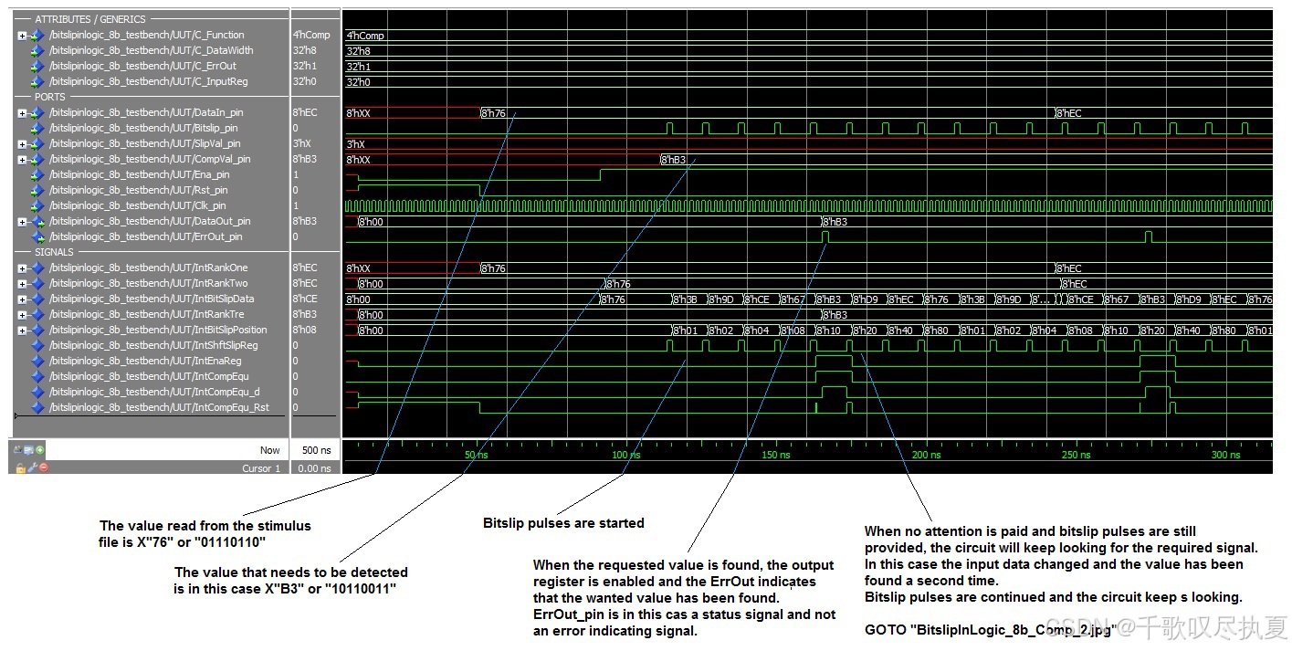
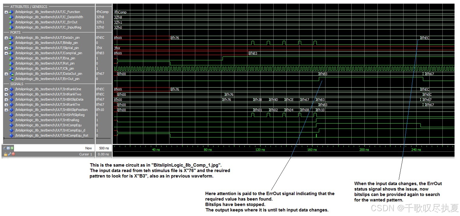
位移位置 0 (IntBitSlipPosition = 00000000, 初始或复位状态):+---+---+---+---+---+---+---+---+| A7| A6| A5| A4| A3| A2| A1| A0| IntRankOne[7:0]+---+---+---+---+---+---+---+---+ | | | | | | | | v v v v v v v v+---+---+---+---+---+---+---+---+| A7| A6| A5| A4| A3| A2| A1| A0| IntBitSlipData+---+---+---+---+---+---+---+---+位移位置 1 (IntBitSlipPosition = 00000001, 第一次位移):+---+ +---+---+---+---+---+---+---+| A0| | B7| B6| B5| B4| B3| B2| B1|+---+ +---+---+---+---+---+---+---+ | | | | | | | | v v v v v v v v+---+---+---+---+---+---+---+---+| A0| B7| B6| B5| B4| B3| B2| B1| IntBitSlipData+---+---+---+---+---+---+---+---+位移位置 2 (IntBitSlipPosition = 00000010, 第二次位移):+---+---+ +---+---+---+---+---+---+| A1| A0| | B7| B6| B5| B4| B3| B2|+---+---+ +---+---+---+---+---+---+ | | | | | | | | v v v v v v v v+---+---+---+---+---+---+---+---+| A1| A0| B7| B6| B5| B4| B3| B2| IntBitSlipData+---+---+---+---+---+---+---+---+位移位置 3 (IntBitSlipPosition = 00000100, 第三次位移):+---+---+---+ +---+---+---+---+---+| A2| A1| A0| | B7| B6| B5| B4| B3|+---+---+---+ +---+---+---+---+---+ | | | | | | | | v v v v v v v v+---+---+---+---+---+---+---+---+| A2| A1| A0| B7| B6| B5| B4| B3| IntBitSlipData+---+---+---+---+---+---+---+---+位移位置 4 (IntBitSlipPosition = 00001000, 第四次位移):+---+---+---+---+ +---+---+---+---+| A3| A2| A1| A0| | B7| B6| B5| B4|+---+---+---+---+ +---+---+---+---+ | | | | | | | | v v v v v v v v+---+---+---+---+---+---+---+---+| A3| A2| A1| A0| B7| B6| B5| B4| IntBitSlipData+---+---+---+---+---+---+---+---+位移位置 5 (IntBitSlipPosition = 00010000, 第五次位移):+---+---+---+---+---+ +---+---+---+| A4| A3| A2| A1| A0| | B7| B6| B5|+---+---+---+---+---+ +---+---+---+ | | | | | | | | v v v v v v v v+---+---+---+---+---+---+---+---+| A4| A3| A2| A1| A0| B7| B6| B5| IntBitSlipData+---+---+---+---+---+---+---+---+位移位置 6 (IntBitSlipPosition = 00100000, 第六次位移):+---+---+---+---+---+---+ +---+---+| A5| A4| A3| A2| A1| A0| | B7| B6|+---+---+---+---+---+---+ +---+---+ | | | | | | | | v v v v v v v v+---+---+---+---+---+---+---+---+| A5| A4| A3| A2| A1| A0| B7| B6| IntBitSlipData+---+---+---+---+---+---+---+---+位移位置 7 (IntBitSlipPosition = 01000000, 第七次位移):+---+---+---+---+---+---+---+ +---+| A6| A5| A4| A3| A2| A1| A0| | B7|+---+---+---+---+---+---+---+ +---+ | | | | | | | | v v v v v v v v+---+---+---+---+---+---+---+---+| A6| A5| A4| A3| A2| A1| A0| B7| IntBitSlipData+---+---+---+---+---+---+---+---+位移位置 8 (IntBitSlipPosition = 10000000, 第八次位移):+---+---+---+---+---+---+---+---+| A7| A6| A5| A4| A3| A2| A1| A0| IntRankOne[7:0]+---+---+---+---+---+---+---+---+ | | | | | | | | v v v v v v v v+---+---+---+---+---+---+---+---+| A7| A6| A5| A4| A3| A2| A1| A0| IntBitSlipData (与位置0相同)+---+---+---+---+---+---+---+---+\"Comp\"模式在找到匹配后不会自动停止位移操作,位移操作完全由外部Bitslip_pin信号控制。然而,它会自动锁定输出为匹配的配置,这是通过IntCompEqu_d寄存器和输出使能逻辑实现的。需要结合自己代码实现training。
布局布线后的框图:
0x76,需要找到0xB3,不停bitslip知道找到0xB3。找到0xB3后,ErrOut_pin拉高,可以从代码看:assign IntCompEqu = (IntBitSlipData == CompVal_pin) ? 1’b1 : 1’b0;
参考设计包含上述两种电路,所选的选项决定了所使用的电路和选项。参考设计是一个可实例化的组件,包含一组可选选项。两种可能的电路各自使用一组选项来应用设计特性。
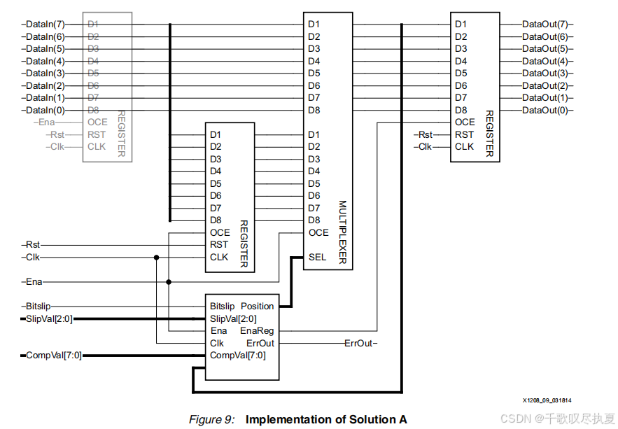
参考设计组件如图 1 所示。引脚功能如下:
• DataIn:4 位或 8 位输入。在 4 位模式下,使用 LSB 半字节。
• BitSlip:控制输入,当脉冲为高电平时,将调用解决方案 A 的 Bitslip 和解决方案 B 的电路使能。
• SlipVal:3 位输入,允许电路在使能输出之前进行定义的 Bitslip 次数。
• CompVal:8 位输入,用于检测数据中的模式。在 4 位模式下,使用 LSB 半字节。
• Ena:电路使能,高电平有效。
• Rst:电路复位,高电平有效。
• Clk:时钟,通常等于 CLKDIV 时钟。
• DataOut:4 位或 8 位输出。在 4 位模式下,使用 LSB 半字节。
• ErrOut:错误和状态输出:
• “Slip” 模式:执行 8 个 Bitslip 后输出高电平脉冲。
• “Nmbr” 模式:表示在执行“Nmbr”个 Bitslip 后输出数据已准备就绪。
• “Comp” 模式:表示检测到请求的模式。
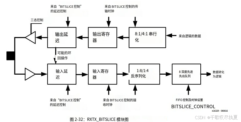
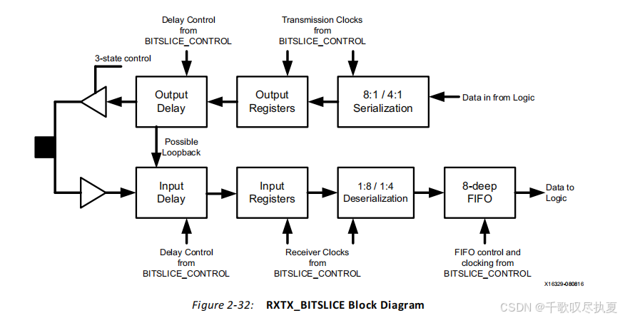
3、RX_BITSLICE功能
补充个概念:
讨论UltraScale(UltraScale+) IO,那就避不开RX_BITSLICE。
在Ultrascale (plus即+)系列上的FPGA中,Xilinx引入了bitslice硬核,它取代了7系列上的IDELAYCTRL/IODELAY/IOSERDES/IODDR系列硬核,用于为HP(High Performance)类型Bank上的IO接口提供串并转化、信号延时、三态控制等功能。Xilinx为bitslice硬核提供了TXRX_BITSLICE/TX_BITSLICE/RX_BITSLICE/BITSLICE_CONTROL/TX_BITSLICE_TRI/RIU_OR 这些与bitslice硬核接口一致的原生原语便于用户直接调用例化。同时为了提供向前兼容性,IDELAYCTRL/IODELAY/IOSERDES/IODDR系列原语作为组件原语仍能继续使用,在综合时会被软件综合为bitslice。
使用bitslice原生原语的优势在于其能够对位于一个字节组上的接口进行批量控制,这对于存储控制器(如DDR)的接口信号时序的优化十分有效。此外bitslice在接收侧增加了一个异步FIFO,便于用户逻辑通过用户时钟读取数据。
官方手册是这样解释功能的:
在本机模式下,RX_BITSLICE包含反序列化逻辑和512分接输入延迟(iddelay),可以连续调整VT变化(这个类似之前的IDELAYCTRL)。RX_BITSLICE包含用于1:4或1:8反序列化的反序列化逻辑,以及允许连接到另一个时钟域的浅FIFO。

RX_BITSLICE模块结构图:


管脚信号,这里就不写了,自己看看ug974。
// RX_BITSLICE : In order to incorporate this function into the design,// Verilog : the following instance declaration needs to be placed// instance : in the body of the design code. The instance name// declaration : (RX_BITSLICE_inst) and/or the port declarations within the// code : parenthesis may be changed to properly reference and// : connect this function to the design. All inputs// : and outputs must be connected.// // RX_BITSLICE: RX_BITSLICE for input using Native Mode // Kintex UltraScale // Xilinx HDL Language Template, version 2022.2 RX_BITSLICE #( .CASCADE(\"FALSE\"), // Enables cascading of IDELAY and ODELAY lines .DATA_TYPE(\"DATA\"), // Defines what the input pin is carrying (CLOCK, DATA, DATA_AND_CLOCK, // SERIAL) .DATA_WIDTH(8), // Defines the width of the serial-to-parallel converter (4-8) .DELAY_FORMAT(\"TIME\"), // Units of the DELAY_VALUE (COUNT, TIME) .DELAY_TYPE(\"FIXED\"), // Set the type of tap delay line (FIXED, VARIABLE, VAR_LOAD) .DELAY_VALUE(0), // Input delay value setting in ps .DELAY_VALUE_EXT(0), // Value of the extended input delay value in ps .FIFO_SYNC_MODE(\"FALSE\"), // Always set to FALSE. TRUE is reserved for later use. .IS_CLK_EXT_INVERTED(1\'b0), // Optional inversion for CLK_EXT .IS_CLK_INVERTED(1\'b0), // Optional inversion for CLK .IS_RST_DLY_EXT_INVERTED(1\'b0), // Optional inversion for RST_DLY_EXT .IS_RST_DLY_INVERTED(1\'b0), // Optional inversion for RST_DLY .IS_RST_INVERTED(1\'b0), // Optional inversion for RST .REFCLK_FREQUENCY(300.0), // Specification of the reference clock frequency in MHz (200.0-2667.0) .SIM_DEVICE(\"ULTRASCALE\"), // Set the device version for simulation functionality (ULTRASCALE) .UPDATE_MODE(\"ASYNC\"), // Determines when updates to the delay will take effect (ASYNC, MANUAL, // SYNC) .UPDATE_MODE_EXT(\"ASYNC\") // Determines when updates to the extended input delay will take effect // (ASYNC, MANUAL, SYNC) ) RX_BITSLICE_inst ( .CNTVALUEOUT(CNTVALUEOUT), // 9-bit output: Counter value to device logic .CNTVALUEOUT_EXT(CNTVALUEOUT_EXT), // 9-bit output: Optional extended (cascaded delay) counter value // going to the device logic .FIFO_EMPTY(FIFO_EMPTY), // 1-bit output: FIFO empty flag .FIFO_WRCLK_OUT(FIFO_WRCLK_OUT), // 1-bit output: FIFO source synchronous write clock out to the device // logic (currently unsupported, do not connect) .Q(Q), // 8-bit output: Registered output data from FIFO .RX_BIT_CTRL_OUT(RX_BIT_CTRL_OUT), // 40-bit output: Output bus to BITSLICE_CONTROL .TX_BIT_CTRL_OUT(TX_BIT_CTRL_OUT), // 40-bit output: Output bus to BITSLICE_CONTROL .CE(CE), // 1-bit input: Clock enable for IDELAY .CE_EXT(CE_EXT), // 1-bit input: Optional extended (cascaded delay) clock enable .CLK(CLK), // 1-bit input: Clock used to sample LOAD, CE, INC .CLK_EXT(CLK_EXT), // 1-bit input: Optional extended (cascaded delay) clock .CNTVALUEIN(CNTVALUEIN), // 9-bit input: Counter value from device logic .CNTVALUEIN_EXT(CNTVALUEIN_EXT), // 9-bit input: Optional extended (cascaded delay) counter value from // device logic .DATAIN(DATAIN), // 1-bit input: Input signal from IBUF .EN_VTC(EN_VTC), // 1-bit input: Enable IDELAYCTRL to keep stable delay over VT .EN_VTC_EXT(EN_VTC_EXT), // 1-bit input: Optional extended (cascaded delay) to keep stable // delay over VT .FIFO_RD_CLK(FIFO_RD_CLK), // 1-bit input: FIFO read clock .FIFO_RD_EN(FIFO_RD_EN), // 1-bit input: FIFO read enable .INC(INC), // 1-bit input: Increment the current delay tap setting .INC_EXT(INC_EXT), // 1-bit input: Optional extended (cascaded delay) increments the // current delay tap setting .LOAD(LOAD), // 1-bit input: Load the CNTVALUEIN tap setting .LOAD_EXT(LOAD_EXT), // 1-bit input: Optional extended (cascaded delay) load the // CNTVALUEIN_EXT tap setting .RST(RST), // 1-bit input: Asynchronous assert, synchronous deassert for // RX_BITSLICE ISERDES .RST_DLY(RST_DLY), // 1-bit input: Reset the internal DELAY value to DELAY_VALUE .RST_DLY_EXT(RST_DLY_EXT), // 1-bit input: Optional extended (cascaded delay) reset delay to // DELAY_VALUE_EXT .RX_BIT_CTRL_IN(RX_BIT_CTRL_IN), // 40-bit input: Input bus from BITSLICE_CONTROL .TX_BIT_CTRL_IN(TX_BIT_CTRL_IN) // 40-bit input: Input bus from BITSLICE_CONTROL ); // End of RX_BITSLICE_inst instantiationRXTX_BITSLICE模块结构图:
除了接收,也有发送或者双向的同样模块:RXTX_BITSLICE。
功能类似,这里不赘述。
// RXTX_BITSLICE : In order to incorporate this function into the design,// Verilog : the following instance declaration needs to be placed// instance : in the body of the design code. The instance name// declaration : (RXTX_BITSLICE_inst) and/or the port declarations within the// code : parenthesis may be changed to properly reference and// : connect this function to the design. All inputs// : and outputs must be connected.// // RXTX_BITSLICE: RXTX_BITSLICE for bidirectional I/O using Native Mode // Kintex UltraScale // Xilinx HDL Language Template, version 2022.2 RXTX_BITSLICE #( .ENABLE_PRE_EMPHASIS(\"FALSE\"), // Enable the pre-emphasis .FIFO_SYNC_MODE(\"FALSE\"), // Always set to FALSE. TRUE is reserved for later use. .INIT(1\'b1), // Defines initial O value .IS_RX_CLK_INVERTED(1\'b0), // Optional inversion for RX_CLK .IS_RX_RST_DLY_INVERTED(1\'b0), // Optional inversion for RX_RST_DLY .IS_RX_RST_INVERTED(1\'b0), // Optional inversion for RX_RST .IS_TX_CLK_INVERTED(1\'b0), // Optional inversion for TX_CLK .IS_TX_RST_DLY_INVERTED(1\'b0), // Optional inversion for TX_RST_DLY .IS_TX_RST_INVERTED(1\'b0), // Optional inversion for TX_RST .RX_DATA_TYPE(\"DATA\"), // Defines what the RX input pin is carrying (CLOCK, DATA, DATA_AND_CLOCK, // SERIAL) .RX_DATA_WIDTH(8), // Defines the width of the serial-to-parallel converter (4-8) .RX_DELAY_FORMAT(\"TIME\"), // Units of the RX DELAY_VALUE (COUNT, TIME) .RX_DELAY_TYPE(\"FIXED\"), // Set the type of RX tap delay line (FIXED, VARIABLE, VAR_LOAD) .RX_DELAY_VALUE(0), // RX Input delay value setting in ps .RX_REFCLK_FREQUENCY(300.0), // Specification of the RX reference clock frequency in MHz (200.0-2667.0) .RX_UPDATE_MODE(\"ASYNC\"), // Determines when updates to the RX delay will take effect (ASYNC, // MANUAL, SYNC) .SIM_DEVICE(\"ULTRASCALE\"), // Set the device version for simulation functionality (ULTRASCALE) .TBYTE_CTL(\"TBYTE_IN\"), // Select between T and TBYTE_IN inputs .TX_DATA_WIDTH(8), // Parallel data input width (4-8) .TX_DELAY_FORMAT(\"TIME\"), // Units of the TX DELAY_VALUE (COUNT, TIME) .TX_DELAY_TYPE(\"FIXED\"), // Set the type of TX tap delay line (FIXED, VARIABLE, VAR_LOAD) .TX_DELAY_VALUE(0), // TX Input delay value setting in ps .TX_OUTPUT_PHASE_90(\"FALSE\"), // Delays the output phase by 90-degrees .TX_REFCLK_FREQUENCY(300.0), // Specification of the TX reference clock frequency in MHz (200.0-2667.0) .TX_UPDATE_MODE(\"ASYNC\") // Determines when updates to the delay will take effect (ASYNC, MANUAL, // SYNC) ) RXTX_BITSLICE_inst ( .FIFO_EMPTY(FIFO_EMPTY), // 1-bit output: FIFO empty flag .FIFO_WRCLK_OUT(FIFO_WRCLK_OUT), // 1-bit output: FIFO source synchronous write clock out to the device // logic (currently unsupported, do not connect) .O(O), // 1-bit output: Serialized output going to output buffer .Q(Q), // 8-bit output: Registered output data from FIFO .RX_BIT_CTRL_OUT(RX_BIT_CTRL_OUT), // 40-bit output: RX Output bus to BITSLICE_CONTROL .RX_CNTVALUEOUT(RX_CNTVALUEOUT), // 9-bit output: RX Counter value from device logic .TX_BIT_CTRL_OUT(TX_BIT_CTRL_OUT), // 40-bit output: Output bus to BITSLICE_CONTROL for TX .TX_CNTVALUEOUT(TX_CNTVALUEOUT), // 9-bit output: TX Counter value to device logic .T_OUT(T_OUT), // 1-bit output: Byte group 3-state output .D(D), // 8-bit input: Data from device logic .DATAIN(DATAIN), // 1-bit input: Input signal from IOBUF .FIFO_RD_CLK(FIFO_RD_CLK), // 1-bit input: FIFO read clock .FIFO_RD_EN(FIFO_RD_EN), // 1-bit input: FIFO read enable .RX_BIT_CTRL_IN(RX_BIT_CTRL_IN), // 40-bit input: RX Input bus from BITSLICE_CONTROL .RX_CE(RX_CE), // 1-bit input: Clock enable for IDELAY .RX_CLK(RX_CLK), // 1-bit input: RX Clock used to sample LOAD, CE, INC .RX_CNTVALUEIN(RX_CNTVALUEIN), // 9-bit input: RX Counter value from device logic .RX_EN_VTC(RX_EN_VTC), // 1-bit input: RX Enable to keep stable delay over VT .RX_INC(RX_INC), // 1-bit input: RX Increment the current delay tap setting .RX_LOAD(RX_LOAD), // 1-bit input: RX Load the CNTVALUEIN tap setting .RX_RST(RX_RST), // 1-bit input: RX Asynchronous assert, synchronous deassert for // RXTX_BITSLICE ISERDES .RX_RST_DLY(RX_RST_DLY), // 1-bit input: RX Reset the internal DELAY value to DELAY_VALUE .T(T), // 1-bit input: Legacy T byte input from device logic .TBYTE_IN(TBYTE_IN), // 1-bit input: Byte group 3-state input from TX_BITSLICE_TRI .TX_BIT_CTRL_IN(TX_BIT_CTRL_IN), // 40-bit input: TX Input bus from BITSLICE_CONTROL .TX_CE(TX_CE), // 1-bit input: Clock enable for ODELAY .TX_CLK(TX_CLK), // 1-bit input: TX Clock used to sample LOAD, CE, INC .TX_CNTVALUEIN(TX_CNTVALUEIN), // 9-bit input: TX Counter value from device logic .TX_EN_VTC(TX_EN_VTC), // 1-bit input: TX Enable to keep stable delay over VT .TX_INC(TX_INC), // 1-bit input: TX Increment the current delay tap setting .TX_LOAD(TX_LOAD), // 1-bit input: TX Load the CNTVALUEIN tap setting .TX_RST(TX_RST), // 1-bit input: TX Asynchronous assert, synchronous deassert for // RXTX_BITSLICE OSERDES .TX_RST_DLY(TX_RST_DLY) // 1-bit input: TX Reset the internal DELAY value to DELAY_VALUE ); // End of RXTX_BITSLICE_inst instantiation4、工程获取
4.1、部分代码
美中不足,xilinx参考代码是VHD写的,顶层文件BitSlipInLogic_Toplevel如下:
----------------------------------------------------------------------------------------------- ____ ____-- / /\\/ /-- /___/ \\ /-- \\ \\ \\/ ?Copyright 2014 Xilinx, Inc. All rights reserved.-- \\ \\ This file contains confidential and proprietary information of Xilinx, Inc.-- / / and is protected under U.S. and international copyright and other-- /___/ /\\ intellectual property laws.-- \\ \\ / \\-- \\___\\/\\___\\------------------------------------------------------------------------------------------------- Device: UltraScale, 7-Series-- Author: Defossez-- Entity Name: BitSlipInLogic_Toplevel-- Purpose: Is same design as Bitslip.vhd but now with front and back-end--registers added. These are added for software timing measurements.--Perform bitslip operations on parallel data.--Extended functionality of native Virtex and 7-Series bitslip.-- Tools: Vivado_2014.1 or newer-- Limitations: none---- Vendor: Xilinx Inc.-- Version: V0.01-- Filename: BitSlipInLogic_Toplevel.vhd-- Date Created: 5 Dec 2014-- Date Last Modified: May 2014----------------------------------------------------------------------------------------------- Disclaimer:--This disclaimer is not a license and does not grant any rights to the materials--distributed herewith. Except as otherwise provided in a valid license issued to you--by Xilinx, and to the maximum extent permitted by applicable law: (1) THESE MATERIALS--ARE MADE AVAILABLE \"AS IS\" AND WITH ALL FAULTS, AND XILINX HEREBY DISCLAIMS ALL--WARRANTIES AND CONDITIONS, EXPRESS, IMPLIED, OR STATUTORY, INCLUDING BUT NOT LIMITED--TO WARRANTIES OF MERCHANTABILITY, NON-INFRINGEMENT, OR FITNESS FOR ANY PARTICULAR--PURPOSE; and (2) Xilinx shall not be liable (whether in contract or tort, including--negligence, or under any other theory of liability) for any loss or damage of any--kind or nature related to, arising under or in connection with these materials,--including for any direct, or any indirect, special, incidental, or consequential--loss or damage (including loss of data, profits, goodwill, or any type of loss or--damage suffered as a result of any action brought by a third party) even if such--damage or loss was reasonably foreseeable or Xilinx had been advised of the--possibility of the same.---- CRITICAL APPLICATIONS--Xilinx products are not designed or intended to be fail-safe, or for use in any--application requiring fail-safe performance, such as life-support or safety devices--or systems, Class III medical devices, nuclear facilities, applications related to--the deployment of airbags, or any other applications that could lead to death,--personal injury, or severe property or environmental damage (individually and--collectively, \"Critical Applications\"). Customer assumes the sole risk and--liability of any use of Xilinx products in Critical Applications, subject only to--applicable laws and regulations governing limitations on product liability.---- THIS COPYRIGHT NOTICE AND DISCLAIMER MUST BE RETAINED AS PART OF THIS FILE AT ALL TIMES.---- Contact: e-mail hotline@xilinx.com phone + 1 800 255 7778----------------------------------------------------------------------------------------------- Revision History:-- Rev. May 2014-- Checked simulations and implementation.-- Reorganise design to fit Olympus and UltraScale, 7-Series XiPhy / ISERDES.----------------------------------------------------------------------------------------------- Naming Conventions:-- Generics start with: \"C_*\"-- Ports-- All words in the label of a port name start with a upper case, AnInputPort.-- Active low ports end in \"*_n\"-- Active high ports of a differential pair end in: \"*_p\"-- Ports being device pins end in _pin \"*_pin\"-- Reset ports end in: \"*Rst\"-- Enable ports end in: \"*Ena\", \"*En\"-- Clock ports end in: \"*Clk\", \"ClkDiv\", \"*Clk#\"-- Signals and constants-- Signals and constant labels start with \"Int*\"-- Registered signals end in \"_d#\"-- User defined types: \"*_TYPE\"-- State machine next state: \"*_Ns\"-- State machine current state: \"*_Cs\"-- Counter signals end in: \"*Cnt\", \"*Cnt_n\"-- Processes: \"_PROCESS\"-- Component instantiations: \"_I__\"---------------------------------------------------------------------------------------------library IEEE; use IEEE.std_logic_1164.all; use IEEE.std_logic_UNSIGNED.all;library UNISIM; use UNISIM.vcomponents.all;library work; use work.all;library Common; use Common.all;----------------------------------------------------------------------------------------------- Entity pin description-- View also PDF documentation in the /Documents Folder-- GENERICS / ATTRIBUTES-- C_Function : \"Slip\" = Normal bitslip. One bit at a time when C_PulsedSlip is 1,-- : else bitslip will happen as long as the BitSlip_Pin is high.-- : \"Nmbr\" = Perform the given amount of bitslips.-- : \"Comp\" = Compare. Auto bitslip until the given value is detected.-- : \"FstC\" = Fast Compare. Different (Low latency) implementation of the -- : compare bitslip solution.-- C_DataWidth : 8, 4-- C_PulsedSlip : If set to 1, bitslip is reduced to a clock period.-- : Leave this at \'1\', unless you are sure that bitslip given by an-- : application is not longer than one Clk_pin cycle.-- C_ErrOut : 1 = ErrOut pin available.-- C_InputReg : 0 = No. Provide an extra input register for the module.---- INPUT / OUTPUT PINS-- DataIn_pin : in : Data input 4 or 8-bit wide.-- Bitslip_pin : in : Perform bitslip when high-- SlipVal_pin : in : Given number of bitslips. For 8-bit this is a 3-bit binary value.-- : For 4-bit this is a 2-bit binary value (Pull MSB bit low)-- CompVal_pin : in : Provided value to compare the input data against.-- Ena_pin : in -- Rst_pin : in -- Clk_pin : in -- DataOut_pin : out 4-bit or 8-bit output data.-- ErrOut_pin : out Error or status depending on C_Function.---------------------------------------------------------------------------------------------entity BitSlipInLogic_Toplevel is generic ( C_Function : string := \"Comp\"; -- Slip, Nmbr, Comp, FstC C_DataWidth : integer := 8; -- 8, 4 C_PulsedSlip : integer := 1; -- 1 = bitslip is reduced to a clock period. -- Leave this at \'1\', unless you are sure that -- a bitslip given by an application is longer -- than one Clk_pin cycle. C_ErrOut : integer := 1; -- 1 = ErrOut pin available. C_InputReg : integer := 0 -- 0, No, 1 = Yes ); port ( DataIn_pin : in std_logic_vector(C_DataWidth-1 downto 0); Bitslip_pin : in std_logic; SlipVal_pin : in std_logic_vector(2 downto 0); CompVal_pin : in std_logic_vector(C_DataWidth-1 downto 0); Ena_pin : in std_logic; Rst_pin : in std_logic; Clk_pin : in std_logic; DataOut_pin : out std_logic_vector(C_DataWidth-1 downto 0); ErrOut_pin : out std_logic );end BitSlipInLogic_Toplevel;----------------------------------------------------------------------------------------------- Architecture section---------------------------------------------------------------------------------------------architecture BitSlipInLogic_Toplevel_arch of BitSlipInLogic_Toplevel is----------------------------------------------------------------------------------------------- Component Instantiation-------------------------------------------------------------------------------------------------------------------------------------------------------------------------------------------- Constants, Signals and Attributes Declarations----------------------------------------------------------------------------------------------- Functions-- Constantsconstant Low : std_logic:= \'0\';constant High : std_logic:= \'1\';-- Signalssignal IntBitslip_pin : std_logic;signal Int_Reg_DataIn_pin : std_logic_vector(C_DataWidth-1 downto 0);signal Int_Reg_Bitslip_pin : std_logic;signal Int_Reg_SlipVal_pin : std_logic_vector(2 downto 0);signal Int_Reg_CompVal_pin : std_logic_vector(C_DataWidth-1 downto 0);signal Int_Reg_Ena_pin : std_logic;signal Int_Reg_Rst_pin : std_logic;signal Int_Reg_DataOut_pin : std_logic_vector(C_DataWidth-1 downto 0);signal Int_Reg_ErrOut_pin : std_logic;-- Attributesattribute KEEP_HIERARCHY : string; attribute KEEP_HIERARCHY of BitSlipInLogic_Toplevel_arch : architecture is \"YES\";attribute LOC : string;---------------------------------------------------------------------------------------------begin----------------------------------------------------------------------------------------------- Input registers---------------------------------------------------------------------------------------------BitSlipInLogic_Toplevel_InReg_PROCESS : process(Clk_pin)begin if (Clk_pin\'event and Clk_pin = \'1\') then Int_Reg_DataIn_pin <= DataIn_pin; Int_Reg_Bitslip_pin <= Bitslip_pin; Int_Reg_SlipVal_pin <= SlipVal_pin; Int_Reg_CompVal_pin <= CompVal_pin; Int_Reg_Ena_pin <= Ena_pin; Int_Reg_Rst_pin <= Rst_pin; end if;end process;----------------------------------------------------------------------------------------------- Output registers---------------------------------------------------------------------------------------------BitSlipInLogic_Toplevel_OutReg_PROCESS : process(Clk_pin)begin if (Clk_pin\'event and Clk_pin = \'1\') then DataOut_pin <= Int_Reg_DataOut_pin; ErrOut_pin <= Int_Reg_ErrOut_pin; end if;end process;----------------------------------------------------------------------------------------------- Generate or not, from a input signal that goes high and stay high a single pulse.-- The input signal can stay high for 1 to n clock cycles, the output will be a -- pulse of the length of a clock period.-----------------------------------------------------------------------------------------Gen_0 : if C_PulsedSlip = 1 generate BitSlipInLogic_Toplevel_I_GenPulsedSlip : entity Common.GenPulse port map (Clk => Clk_pin, Ena => High, SigIn => Int_Reg_Bitslip_pin, SigOut => IntBitslip_pin);end generate Gen_0;--Gen_1 : if C_PulsedSlip = 0 generate IntBitslip_pin <= Bitslip_pin;end generate Gen_1;-----------------------------------------------------------------------------------------Gen_2 : if C_DataWidth = 8 generate Gen_2_0 : if C_Function /= \"FstC\" generate BitSlipInLogic_Toplevel_I_Btslp8b : entity work.BitSlipInLogic_8b generic map ( C_Function => C_Function, -- Slip, Nmbr, Comp C_ErrOut => C_ErrOut, -- 1 = ErrOut pin available. C_InputReg => C_InputReg -- 0, No, 1 = Yes ) port map ( DataIn_pin => Int_Reg_DataIn_pin, -- in [7:0] Bitslip_pin => IntBitslip_pin, -- in SlipVal_pin => Int_Reg_SlipVal_pin(2 downto 0), -- in [2:0] CompVal_pin => Int_Reg_CompVal_pin, -- in [7:0] Ena_pin => Int_Reg_Ena_pin, -- in Rst_pin => Int_Reg_Rst_pin, -- in Clk_pin => Clk_pin, -- in DataOut_pin => Int_Reg_DataOut_pin, -- out [7:0] ErrOut_pin => Int_Reg_ErrOut_pin ); end generate Gen_2_0; -- Gen_2_1 : if C_Function = \"FstC\" generate BitSlipInLogic_Toplevel_I_BtslpFstC8b : entity work.BitSlipInLogic_FstCmp_8b generic map ( C_Function => C_Function, -- FstC, -- C_ErrOut => C_ErrOut, -- 1 = ErrOut pin available., -- C_InputReg => C_InputReg -- 0, No, 1 = Yes -- ) port map ( DataIn_pin => Int_Reg_DataIn_pin, -- in [7:0] Bitslip_pin => IntBitslip_pin, -- in CompVal_pin => Int_Reg_CompVal_pin, -- in [7:0], Ena_pin => Int_Reg_Ena_pin, -- in, -- in Rst_pin => Int_Reg_Rst_pin, -- in, -- in Clk_pin => Clk_pin, -- in, -- in DataOut_pin => Int_Reg_DataOut_pin, -- out [7:0], ErrOut_pin => Int_Reg_ErrOut_pin -- out ); end generate Gen_2_1;end generate Gen_2;-----------------------------------------------------------------------------------------Gen_3 : if C_DataWidth = 4 generate Gen_3_0 : if C_Function /= \"FstC\" generate BitSlipInLogic_Toplevel_I_Btslp4b : entity work.BitSlipInLogic_4b generic map ( C_Function => C_Function, -- Slip, Nmbr, Comp C_ErrOut => C_ErrOut, -- 1 = ErrOut pin available. C_InputReg => C_InputReg -- 0, No, 1 = Yes ) port map ( DataIn_pin => Int_Reg_DataIn_pin, -- in [3:0] Bitslip_pin => IntBitslip_pin, -- in SlipVal_pin => Int_Reg_SlipVal_pin(1 downto 0), -- in [1:0] CompVal_pin => Int_Reg_CompVal_pin, -- in [3:0] Ena_pin => Int_Reg_Ena_pin, -- in Rst_pin => Int_Reg_Rst_pin, -- in Clk_pin => Clk_pin, -- in DataOut_pin => Int_Reg_DataOut_pin, -- out [3:0] ErrOut_pin => Int_Reg_ErrOut_pin ); end generate Gen_3_0; -- Gen_3_1 : if C_Function = \"FstC\" generate BitSlipInLogic_Toplevel_I_BtslpFstC4b : entity work.BitSlipInLogic_FstCmp_4b generic map ( C_Function => C_Function, -- FstC, -- C_ErrOut => C_ErrOut, -- 1 = ErrOut pin available., -- C_InputReg => C_InputReg -- 0, No, 1 = Yes -- ) port map ( DataIn_pin => Int_Reg_DataIn_pin, -- in [3:0] Bitslip_pin => IntBitslip_pin, -- in CompVal_pin => Int_Reg_CompVal_pin, -- in [3:0], Ena_pin => Int_Reg_Ena_pin, -- in, -- in Rst_pin => Int_Reg_Rst_pin, -- in, -- in Clk_pin => Clk_pin, -- in, -- in DataOut_pin => Int_Reg_DataOut_pin, -- out [3:0], ErrOut_pin => Int_Reg_ErrOut_pin -- out ); end generate Gen_3_1;end generate Gen_3;end BitSlipInLogic_Toplevel_arch;--4.2、完整工程(含仿真)
https://download.csdn.net/download/weixin_46423500/90841574
总结
本文主要学习并描述Xilinx UltraScale+ bitslip实现的2个方案,后续会根据这2个方案,自己设计一个新的DDR bitslip方案。 届时,再重启一篇文章进行分享。


